MCS series magnification standards
EM-Tec MCS series magnification calibration standards from Micro to Nano are unique, cost effective, wide ranging SEM calibration standards. They can be used for magnification calibration or critical dimension measurements in table top SEM, standard SEM, FESEM, FIB, Auger, SIMS and reflected light microscope systems.
Two types of calibration ranges for the EM-Tec MCS calibration standards are available, both standard with certificates of traceability or optionally with an individual certificate of calibration:
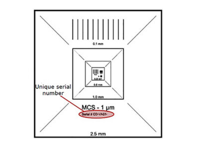
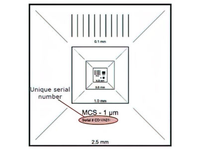
- EM-Tec MCS-1 with a scale ranging from 2.5mm to 1µm – ideal for table top and compact SEMs and cover 10x to 20,000x magnifications. Available as a traceable or fully certified version.
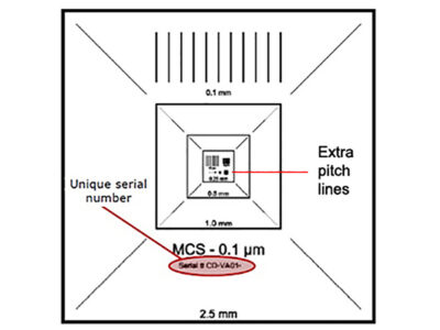
- EM-Tec MCS-0.1 with a scale ranging from 2.5mm down to 100nm – ideal for SEM, FESEM and FIB systems and cover 10x to 200,000 magnifications. Available as a traceable or fully certified version.
The Micro to NanoEM-Tec MCS-0.1 calibration standard is an excellent replacement for the discontinued SIRA calibration standard (which was using only 0.51 and 0.463µm features) with added advantages. Compatible feature sizes for the SIRA standard are 50µm (5 x 10µm) and 0.5µm (500nm).
EM-Tec MCS series are made using state-of-the-art MEMS manufacturing techniques with high contrast chromium deposited lines for the larger features and gold-over-chromium for smaller features below 2.5µm The gold layer ensures an optimum signal-to-noise ratio for calibration purposes.
Advantages of the EM-Tec MCS series are:
- Unprecedented precision over the full calibration range
- All features in one single ultra flat plane
- Metal on silicon with excellent signal to noise ratio
- Wider range of features to accurately calibrate low, medium and high magnification ranges
- Compatible with both SE and BSE imaging
- Fully conductive materials
- Easy to convert feature sizes
- Can be cleaned with plasma cleaning
- All NIST traceable or optionally certified

Substrate
525µm thick boron doped ultra-flat wafer with <100> orientation
Conductivity
Excellent – 5-10 Ohm resistivity
Pattern size
3 x 3mm
Pitch/precision
1µm ± 0.025µm, 10µm ± 0.025µm and 100µm ± 0.25µm
Line type / depth
Etched in Si, 300nm ± 30nm deep lines
Line width
200nm ± 10nm for 1µm pitch lines
300nm ± 15nm for 10µm pitch lines
400nm ± 20nm for 100 µm pitch lines
Perpendicularity
Better than 0.01°
Markers
Edge fiducial markers for grid position finding
Die size
4 x 4mm
Application
SEM, FESEM, FIB, Auger, SIMS and reflected light microscopy
Identification
Product ID with serial number etched
Mounting
Unmounted, mounting optionally available
Supplied
Supplied in a Gel-Pak box
Certification
Wafer level certificate of traceability to NIST
Example of individual certificate of calibration for the EM-Tec MCS certified magnification calibration standard
Ordering information:
-
Certified calibration standard 2.5mm-100nm, on a 12.7mm pin
EM-Tec MCS-0.1CF certified calibration standard, 2.5mm to 100nm – mounted on standard 12.7mm pin (each)
£960.00 Add to basket -
Certified calibration standard 2.5mm-100nm on 12.7mm pin
EM-Tec MCS-0.1CF certified calibration standard, 2.5mm to 100nm – mounted on Zeiss 12.7mm pin stub (each)
£960.00 Add to basket -
Certified calibration standard 2.5mm-100nm on a JEOL stub
EM-Tec MCS-0.1CF certified calibration standard- 2.5mm to 100nm- mounted on 12.2mm JEOL stub (each)
£975.00 Add to basket -
Certified calibration standard 2.5mm-100nm on a Hitachi stub
EM-Tec MCS-0.1CF certified calibration standard, 2.5mm to 100nm – mounted on 15mm Hitachi stub (each)
£960.00 Add to basket -
Traceable calibration standard 2.5mm-100nm on a 12.7mm pin
EM-Tec MCS-0.1TR traceable calibration standard, 2.5mm to 100nm, mounted on standard 12.7mm pin (each)
£418.00 Add to basket -
Traceable calibration standard 2.5-100nm on a Zeiss pin stub
EM-Tec MCS-0.1TR traceable calibration standard, 2.5mm to 100nm – mounted on Zeiss 12.7mm pin stub (each)
£418.00 Add to basket -
Traceable calibration standard 2.5mm-100nm on a JEOL stub
EM-Tec MCS-0.1TR traceable calibration standard, 2.5mm to 100nm – mounted on 12.2mm JEOL stub (each)
£435.00 Add to basket -
Traceable calibration standard 2.5mm-100nm on a Hitachi stub
EM-Tec MCS-0.1TR traceable calibration standard, 2.5mm to 100nm – mounted on 15mm Hitachi stub (each)
£418.00 Add to basket -
Traceable calibration standard 2.5mm to 100nm unmounted
M-Tec MCS-0.1TR traceable calibration standard, 2.5mm to 100nm, unmounted (each)
£407.00 Add to basket -
Certified calibration standard 2.5mm to 100nm, unmounted
EM-Tec MCS-0.1CF certified calibration standard, 2.5mm to 100nm -unmounted (each)
£939.00 Add to basket
-
Certified calibration standard, 2.5mm to 1µm on a 12.7mm pin
EM-Tec MCS-1CF certified calibration standard, 2.5mm to 1µm – mounted on standard 12.7mm pin (each)
£635.00 Add to basket -
Certified calibration standard, 2.5mm to 1µm on a 12.7mm pin
EM-Tec MCS-1CF certified calibration standard, 2.5mm to 1µm – mounted on Zeiss 12.7mm pin stub (each)
£635.00 Add to basket -
Certified calibration standard, 2.5mm to 1µm on a JEOL stub
EM-Tec MCS-1CF certified calibration standard, 2.5mm to 1µm – mounted on 12.2mm JEOL stub (each)
£650.00 Add to basket -
Certified calibration standard- 2.5mm-1µm on Hitachi stub
EM-Tec MCS-1CF certified calibration standard, 2.5mm to 1µm – mounted on 15mm Hitachi stub (each)
£635.00 Add to basket -
Certified calibration standard, 2.5mm to 1µm, unmounted
EM-Tec MCS-1CF certified calibration standard, 2.5mm to 1µm – unmounted (each)
£624.00 Add to basket -
Traceable calibration standard 2.5mm-1µm on a 12.7mm stub
EM-Tec MCS-1TR traceable calibration standard, 2.5mm to 1µm, mounted on standard 12.7mm pin (each)
£94.00 Add to basket -
Traceable calibration standard 2.5mm-1µm on a Zeiss pin stub
EM-Tec MCS-1TR traceable calibration standard, 2.5mm to 1µm – mounted on Zeiss 12.7mm pin stub (each)
£94.00 Add to basket -
Traceable calibration standard 2.5mm-1µm on a JEOL stub
EM-Tec MCS-1TR traceable calibration standard, 2.5mm to 1µm – mounted on 12.2mm JEOL stub (each)
£100.00 Add to basket -
Traceable calibration standard 2.5mm-1µm on a Hitachi stub
EM-Tec MCS-1TR traceable calibration standard, 2.5mm to 1µm – mounted on 15mm Hitachi stub (each)
£94.00 Add to basket -
Traceable calibration standard 2.5mm to 1µm unmounted
EM-Tec MCS-1TR traceable calibration standard, 2.5mm to 1µm, unmounted (each)
£84.00 Add to basket