Platinum coated silicon and glass substrates
Platinium coated substrates are available as a Ø 4”/100mm silicon wafer, 10 x 10mm silicon chips, microscope slide and coverslips. Substrates are coated with100nm of pure platinum (99.99%). They are useful for thin film research, MEMs, sensors, nanotechnology, and biotechnology applications. Platinum coatings exhibit high conductance and high corrosion resistance. An adhesion layer of titanium is deposited between the substrate and the platinium coating.
Both titanium and platinium coatings are deposited in a dedicated high vacuum deposition system using an electron beam (EB) source. The platinum coating is not atomically flat – there are height differences in the nanometre range. For protection, the wafers are packed in wafer carrying trays, the silicon chips and glass coverslips are in Gel-Pak boxes. The slides are packed in slide mailers.
")


Specifications of platinium coated substrates
| Platinum coating |
100 nm Pt (99.99% purity) |
|||
| Titanium adhesion film |
5 nm Ti (99.99% purity) |
|||
| Surface roughness |
Several nm |
|||
| Substrate |
Silicon wafer |
Si chips |
Microscope slide |
Coverslip |
| Dimensions |
Ø 4” / 100 mm |
10 x 10 mm |
75 x 25 mm |
22 x 22 mm |
| Thickness |
525 µm (+/- 20 µm |
1 mm |
0.2 mm |
|
| Material type |
P (Boron) – <100> – 1-30 Ohm/cm |
Borofloat 33 – borosilicate glass |
||
Ordering information:
-
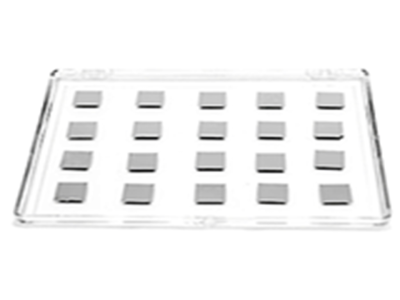
Platinum coated coverslip, 22 x22x 0.2 mm, 100nm Pt
Nano-Tec platinum coated coverslip, 22 x22x 0.2 mm, 100nm Pt (Pk/20)
£1,166.00 Add to basket -
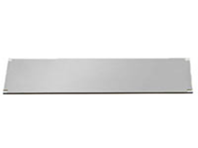
Platinum (Pt) coated microscope slide, 75x25x1 mm, 100nm
Nano-Tec platinum coated microscope slide, 75x25x1 mm, 100nm Pt (Pk/5)
£558.00 Add to basket -
Platinum (Pt) coated silicon chips, 10 x 10 mm, 525µm thick, 100nm
Nano-Tec platinum coated silicon chips, 10 x 10 mm, 525µm thickness, 100nm Pt (Pk/20)
£535.00 Add to basket -
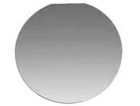
Platinum coated silcon wafer, Ø4inch / 100mm, 525µm thick, 100nm Pt
Nano-Tec platinum coated silicon wafer, Ø4inch / 100mm, 525µm thickness, 100nm Pt (each)
£392.00 Add to basket