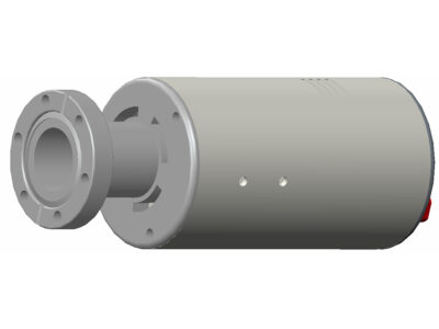
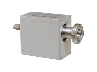
SEMI-KLEEN Sapphire downstream RF plasma cleaner
SEMI-KLEEN Sapphire is a remote plasma cleaner designed to meet the rigorous requirements of the semiconductor industry. It is designed for applications where NF3, CF4 type corrosive gases are to be used.
It can be used on the following instruments: electron beam review systems (EBR), electron beam inspection systems (EBI) CD-SEM, electron beam lithography systems, EUV lithography (EUVL) and EUV mask inspectors.
- Highly resistant sapphire tube – optimised for use with aggressive and corrosive gases
- Specifically designed for semiconductor applications
- Advanced, dual-stage particle filtering technology
- Low particulate high reliability plasma source design
- Instant plasma ignition at extremely low pressures
- Probe monitoring of the plasma strength – guides user to set optimal recipes
- Two year warranty
SEMI-KLEEN Sapphire remote plasma cleaner is an enhanced version of the SEMI-KLEEN Quartz plasma cleaner. A more chemically resistant sapphire tube replaces the standard quartz chamber and is designed to be resistant to aggressive and corrosive process gases. In addition, the vacuum seal and chamber material have been optimised to support corrosive radicals inside the plasma chamber. For plasma cleaning applications where hydrogen plasma etching of quartz chamber is a concern, the SEMI-KLEEN Sapphire is a better choice over the traditional quartz chamber hydrogen plasma source.
Apart from the addition of the sapphire tube, the specification of the SEMI-KLEEN Sapphire is identical to the standard SEMI-KLEEN Quartz – for details please see: SEMI-KLEEN Quartz.

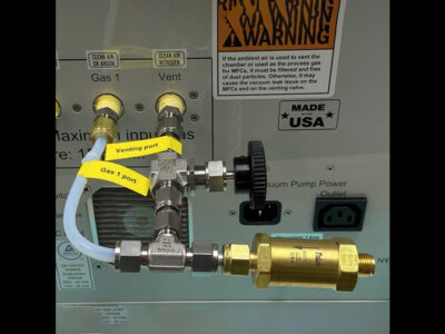
Application example
SEMI-KLEEN Sapphire was used to deposit thin films and to clean specimen surfaces prior to thin film deposition in atomic layer deposition systems and to clean carbon and oxygen contaminations from metal surfaces. The results show that SEMI-KLEEN Sapphire can clean carbon and oxygen contaminants from InGaAs specimens with using only a two second hydrogen plasma. Highly efficient hydrogen plasma sources require low pressure discharge capabilities, otherwise atomic hydrogen will recombine and lose its effectiveness.
XPS analysis of contaminated InGaAs specimen before and after two second hydrogen plasma cleaning

Upgrade of SEMI-KLEEN Sapphire to UHV compatibility
Option PIE-SEMI106 upgrades the standard SEMI-KLEEN for use with UVH systems. This consists of a quartz glass tube brazed to the stainless-steel flange, CF2.75″ front flange and a 1/4″ VCR gas connector on the rear of the instrument. There is no internal pressure sensor or internal gas flow controller.
For other instruments in the PIE Scientific KLEEN range and for Tergeo bench top plasma cleaners please see here: KLEEN & Tergeo.
PIE-SEM101. Upgrade to CF2.75″ flange
PIE-SEM102. Rack mounted controller
PIE-SEM103. 3nm particle filter
PIE-SEMI105. Upgrade to 150W RF power supply
PIE-SEMI106. Upgrade to SEMI-KLEEN UHV
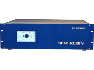
SEMI-KLEEN plasma cleaner
- Tabletop controller with embedded microcomputer and LCD touchscreen user interface
- Low particle source design, qualified for semiconductor application where PWP is a concern.
- PC remote control software with intuitive user interface
- 60-recipe support in microcontroller
- 75W RF power supply with fixed RF impedance matching (IE-SEMI105. Upgrade to 150W RF power supply)
- Plasma sensor for plasma strength monitor
- Electronic gas flow control with pressure sensor feedback control
- Smart-Schedule feature for automatic cleaning
- Intelligent safe and expert operation mode 15 feet high-quality, high-power RF cable; D-Sub 9 PC control cable; D-Sub 15 source control cable
A radio frequency (RF) plasma is an ionised gas phase substance that consists of ions, electrons, and neutral atoms and/or molecules that grossly maintain charge neutrality. Electrons and ions should be close enough so that each of them can influence many nearby charged particles within a radius called the Debye screening length. As a result, charged particles in the RF plasma respond collectively to external electromagnetic fields. With a high density of free-moving ions and electrons, plasma is highly electrically conductive. With the exception of boundary regions between the plasma and electrodes, a plasma contains the same amount of positive and negative charges. There is no space charge within the bulk of the plasma.
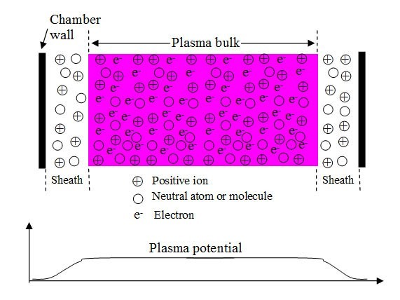
Plasma sheath
Electron temperature is usually equal to or higher than that of ions. Since electrons are much lighter than ions, they can escape from a plasma at a much faster speed than ions, providing there is no confining potential barrier. Once electrons are nearly depleted from the boundary interface between the plasma and electrodes or specimen, a region with only positive ions and neutrals will be formed. This usually dark boundary region is called plasma sheath. Positive charges in the plasma sheath can push more ions to diffuse out of the plasma. It also creates a potential barrier to prevent electrons from diffusing out of the plasma. Eventually, the loss rate of electrons and ions will reach an equilibrium state. The plasma sheath also creates a positive plasma potential with respect to the grounded chamber walls. The voltage drop across the plasma sheath can accelerate ions and create an ion sputtering effect in many applications.
How an RF plasma is generated
Electrons and ions in plasmas can disappear through diffusion or recombination. To sustain a stable RF plasma, external excitation is required to create more electrons and ions so that their creation rate can reach a balance with the loss rate. Most RF plasma generation methods rely on heating free electrons to high enough energy to break down neutral atoms or molecules into ions and electrons.
PIE Scientific specialise in developing advanced plasma systems for plasma etching, cleaning, surface treatment, ion and electron beam production applications. The company was founded by alumni of the Plasma and Ion Source Technology group in the Lawrence Berkeley National Laboratory. After 15 years of experience in developing advanced semiconductor capital equipment in Silicon Valley, they realized that many existing low-cost plasma cleaners and plasma treatment systems were still using decades-old technology. Therefore, they decided to bring state-of-the-art plasma technology developed for the semiconductor industry and nuclear research into affordable plasma instruments. Their SmartClean™ technology has been well-received by customers.
Ordering information:

Options and accesories for SEMI-KLEEN
-
Upgrade to CF2.75″ flange
Upgrade to CF2.75″ flange
Price On Request Read more -
Rack mounted controller
Rack mounted controller
Price On Request Read more -
Particle filter 3nm
3nm particle filter
Price On Request Read more -
Sapphire tube option for NF3 CF4 type corrosive gases
Sapphire tube option for NF3 CF4-type corrosive gases
Price On Request Read more -
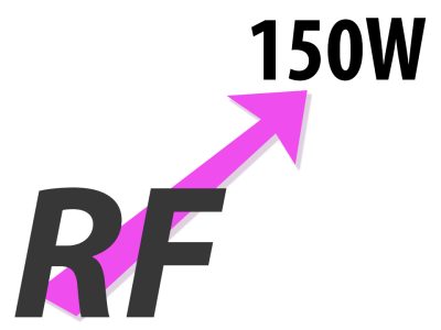
Upgrade from standard 75W to 150W RF power supply
Option to upgrade to 150W RF power supply
Price On Request Read more